(China (Mainland))

Product Summary
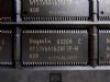
The SST34HF1681J-70-4E-L1PE is an 8 Mbit PSRAM ComboMemory integrated either a 1M x16 or 2M x8 CMOS flash memory bank with either a 256K x16, or 512K x16 CMOS pseudo SRAM (PSRAM) memory bank in a multi-chip package (MCP). The device is fabricated using SST’s proprietary, high-performance CMOS SuperFlash technology incorporating the split-gate cell design and thick-oxide tunneling injector to attain better reliability and manufacturability compared with alternate approaches. The SST34HF1681J-70-4E-L1PE is ideal for applications such as cellular phones, GPS devices, PDAs, and other portable electronic devices in a low power and small form factor system.
Parametrics
SST34HF1681J-70-4E-L1PE absolute maximum ratings: (1)Operating Temperature: -20℃ to +85℃; (2)Storage Temperature: -65℃ to +125℃; (3)D. C. Voltage on Any Pin to Ground Potential: -0.5V to VDD +0.3V; (4)1. VDD = VDDF and VDDS; (5)Transient Voltage (<20 ns) on Any Pin to Ground Potential: -1.0V to VDD +1.0V; (6)Package Power Dissipation Capability (TA= 25℃): 1.0W; (7)Surface Mount Solder Reflow Temperature: 260℃ for 10 seconds; (8)Output Short Circuit Current: 50 mA.
Features
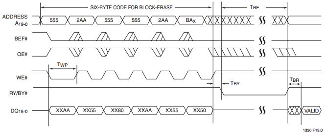
SST34HF1681J-70-4E-L1PE features: (1)Flash Organization: 1M x16 or 2M x8; (2)Dual-Bank Architecture for Concurrent Read/Write Operation, Bottom Sector Protection; 16 Mbit: 12 Mbit + 4 Mbit; (3)PSRAM Organization: 4 Mbit: 256K x16; 8 Mbit: 512K x16; (4)Single 2.7-3.3V Read and Write Operations; (5)Superior Reliability, Endurance: 100,000 Cycles (typical); Greater than 100 years Data Retention; (6)Low Power Consumption: Active Current: 25 mA (typical); PSRAM Standby Current: 40 μA (typical); (7)Hardware Sector Protection (WP#), Protects 4 outer most sectors (4 KWord) in the larger bank by holding WP# low and unprotects by holding WP# high ; (8)Hardware Reset Pin (RST#), Resets the internal state machine to reading data array; (9)Byte Selection for Flash (CIOF pin), Selects 8-bit or 16-bit mode (56-ball package only); (10)Sector-Erase Capability, Uniform 2 KWord sectors; (11)Block-Erase Capability, Uniform 32 KWord blocks; (12)Read Access Time, Flash: 70 ns; PSRAM: 70 ns; (13)Erase-Suspend / Erase-Resume Capabilities; (14)Security ID Feature, SST: 128 bits; User: 128 bits; (15)Latched Address and Data; (16)Fast Erase and Program (typical): Sector-Erase Time: 18 ms; Block-Erase Time: 18 ms; Chip-Erase Time: 35 ms; Program Time: 7 μs; (17)Automatic Write Timing, Internal VPPGeneration; (18)End-of-Write Detection, Toggle Bit; Data# Polling; Ready/Busy# pin; (19)CMOS I/O Compatibility; (20)JEDEC Standard Command Set; (21)Packages Available, 56-ball LFBGA (8mm x 10mm); 62-ball LFBGA (8mm x 10mm); (22)All non-Pb (lead-free) devices are RoHS compliant.
Diagrams
| Image | Part No | Mfg | Description |  |
Pricing (USD) |
Quantity | ||||
|---|---|---|---|---|---|---|---|---|---|---|
 |
 SST34HF1681J-70-4E-L1PE |
Greenliant |
Flash 16M Flash 8M SRAM Extended Temp |
Data Sheet |
Negotiable |
|
||||
| Image | Part No | Mfg | Description | |
Pricing (USD) |
Quantity | ||||
|
SST308 |
Vishay/Siliconix |
JFET 35V 12mA |
Data Sheet |
Negotiable |
|
||||
|
SST308-E3 |
Vishay/Siliconix |
JFET 35V 12mA |
Data Sheet |
Negotiable |
|
||||
|
SST308-T1 |
Vishay/Siliconix |
JFET 35V 12mA |
Data Sheet |
Negotiable |
|
||||
|
SST308-T1-E3 |
Vishay/Siliconix |
JFET 35V 12mA |
Data Sheet |
Negotiable |
|
||||
|
SST309 |
Vishay/Siliconix |
JFET 35V 12mA |
Data Sheet |
Negotiable |
|
||||
|
SST309-E3 |
Vishay/Siliconix |
JFET 35V 12mA |
Data Sheet |
Negotiable |
|
||||