(China (Mainland))

Product Summary
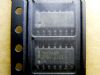
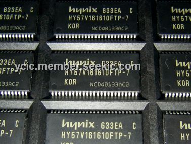
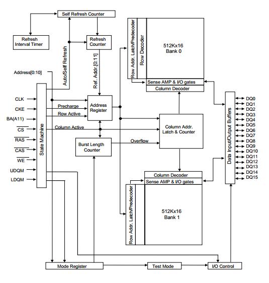
The HY57V161610FTP-7 is a 16,777,216-bits CMOS Synchronous DRAM, ideally suited for the main memory and graphic applications which require large memory density and high bandwidth. The HY57V161610FTP-7 is organized as 2banks of 524,288x16. The device is offering fully synchronous operation referenced to a positive edge clock. All inputs and outputs are synchronized with the rising edge of the clock input. The data paths are internally pipelined to achieve very high bandwidth. All input and output voltage levels are compatible with LVTTL.
Parametrics
HY57V161610FTP-7 absolute maximum ratings: (1)Ambient Temperature, TA: 0 to 70℃; (2)Storage Temperature, TSTG: -55 to 125℃; (3)Voltage on Any Pin relative to VSS, VIN, VOUT: -1.0 to 4.6 V; (4)Voltage on VDDrelative to VSS, VDD: -1.0 to 4.6 V; (5)Short Circuit Output Current, IOS: 50 mA; (6)Power Dissipation, PD: 1W; (7)Soldering Temperature·Time, TSOLDER: 260·10℃·Sec.
Features
HY57V161610FTP-7 features: (1)Single 3.0V to 3.6V power supply; (2)All device pins are compatible with LVTTL interface; (3)JEDEC standard 400mil 50pin TSOP-II with 0.8mm of pin pitch; (4)All inputs and outputs referenced to positive edge of system clock; (5)Data mask function by UDQM/LDQM; (6)Internal two banks operation; (7)Auto refresh and self refresh; (8)4096 refresh cycles / 64ms; (9)Programmable Burst Length and Burst Type, 1, 2, 4, 8 and Full Page for Sequence Burst; 1, 2, 4 and 8 for Interleave Burst; (10)Programmable CASLatency; 1, 2, 3 Clocks.
Diagrams
 |
 HY57V658020B |
Other |
|
Data Sheet |
Negotiable |
|
||||
|
HY57V641620E(S)T(P)-xI |
Other |
|
Data Sheet |
Negotiable |
|
||||
|
HY57V641620E(L)T(P)-xI |
Other |
|
Data Sheet |
Negotiable |
|
||||
|
HY57V56820CT |
Other |
|
Data Sheet |
Negotiable |
|
||||
|
HY57V56820CL |
Other |
|
Data Sheet |
Negotiable |
|
||||
|
HY57V561620T |
Other |
|
Data Sheet |
Negotiable |
|
||||